
A voltage inverter circuit
Our programmable MP3 player has an interface to an LCD with a HD44780 controller. These are alphanumeric LCDs with one to 4 lines of text and 16 to 40 characters per line. However, these LCDs (and LCDs in general) exist in two varieties: those that require a positive LC-driving voltage and those that need a negative LC-driving voltage. The H0420 (the programmable MP3 player that I referred to earlier) only supports LCDs with a positive LC-driving voltage, because it takes its power directly from a common (asymetric) mains power adapter.
A voltage inverter (that creates a negative tension from a positive one) would enable you to connect an LCD with a negative LC-driving voltage to the H0420. The (negative) output voltage must be adjustable because the optimal LC-driving voltage depends on the view angle and the temperature. The H0420 already has a pin for a positive LC-driving voltage between 0V and +5V. Our circuit must "intercept" this pin and modify it to produce a negative voltage.
The circuit
The image below shows the voltage inverter circuit, which is centred around the well known 555 timer chip. The schematic consists of three parts: an oscillator that converts DC in AC, a special kind of rectifier that converts AC to DC (but now negative), and a voltage regulator. None of the component values is critical, by the way.
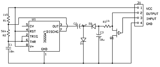
The 555 timer chip is wired as an oscillator. As is covered in detail in many books and articles, the "high period" of the cycle takes 0.693×(R1+R2)×C1 seconds and the low period takes 0.693×R2×C1 seconds. With the values of R1, R2 and C1, this produces a nearly square wave at roughly 1.3 kHz at pin 3.
The two diodes look like half of a rectifier bridge and indeed they do produce a DC signal, but in a different way than the common diode bridges. When pin 3 of the 555 is high, diode D1 conducts (and diode D2 blocks) and thereby the 555 charges capacitor C2. When pin 3 toggles low, D1 blocks. There is still a charge in C2 and the "+" side of the capacitor is now the zero-volt level (because pin 3 is temporarily at zero volt). The other side must then be minus VCC, if I am allowed to ignore the threshold of D1 for the moment. That, in turn, means that diode D2 conducts and that C2 charges C3... with a negative voltage. Capacitor C3 functions as a smoothing capacitor.
As said, the output tension must be controllable (i.e. adjustable). An easy way to do so is to make an adjustable voltage divider with one fixed resistor and one variable resitor. This is the combination of R3 and Q1; Q1 is a P-channel junction FET, for which I have used the J175.
End notes
Due to the voltage threshold of the diodes, the output range is from zero volt to approximately -3.8V (with Vcc at 5V). The relation to the control voltage (input in the schematic) and the output voltage is not linear. This was not important for my application, but it needs to be mentioned.
Before arriving at this circuit, I have tried to use the control voltage as Vcc, and drop R3 and Q1. However, in the design of the H0420, the LC-driving voltage pin could not produce sufficient current to feed the 555 chip. In addition, the standard 555 needs a power supply of at least 4.5V. There are alternative implementations of the 555: a low-power CMOS version of the 555 would comply with the current supply of the LC-driving voltage pin of the H0420, and versions that work on 3V exist too. I have not tried these, but opted instead for the R3/Q1 voltage divider and a stable Vcc of 5V.
This circuit fits on a piece of experimation board of 12 by 5 pins with normal components. You can make it smaller with a custom PCB, and smaller still by using SMD components. I have put the PCB directly in the ribbon cable that links the LCD to the H0420 (the ground, VCC and LC-driving voltage pins are close together in the ribbon cable).
