

Reflow soldering profiles
These guidelines apply specifically for "batch" ovens (also called bench-top ovens or furnace-style ovens). The temperature profile is in part mandated by the (mechanical) design of the oven, and batch ovens have a radically different design than conveyor belt ovens.
In particular, these guidelines apply to the “eC-reflow-mate” reflow oven from Eurocircuits.
A particular difference is the influence of thermal inertia. Thermal inertia exists in the oven itself and in the PCB (and the components). In a conveyor belt oven, the PCB physically moves through the different heating zones in the oven, and therefore, the thermal inertia of these heating zones have little implication on the PCB (once a PCB is out of the oven, it does not matter any more how long the oven stays hot).
In a conveyor belt oven, the distance between the heating zones is fixed and the conveyor belt runs through all zones —and therefore, the PCBs move through all zones with the same speed. The difficulty of calibrating a profile for a conveyor belt oven is that a change in the parameter for one zone typically influences the characteristics of the other zones. In comparison, a batch oven allows for some flexibility in the profiles. That said, because of the relatively large thermal inertia, the actual temperature curve deviates from the (theoretical) profile.
The solution, then, is to anticipate the thermal inertia in the profile. The knowledge required to make these decisions must be obtained with actual measurements.
Characteristics of the “eC-reflow-mate”
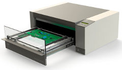 The Eurocircuits eC-reflow-mate
is a batch oven with quartz infra-red heaters on the top and bottom plus convection
(controlled air flow). The oven has two floating temperature sensors (top and bottom)
and a provision for one sensor to clamp/attach onto the PCB (the “external”
sensor).
The Eurocircuits eC-reflow-mate
is a batch oven with quartz infra-red heaters on the top and bottom plus convection
(controlled air flow). The oven has two floating temperature sensors (top and bottom)
and a provision for one sensor to clamp/attach onto the PCB (the “external”
sensor).
Eurocircuits documents that the infra-red lamps take 20 to 30 seconds to heat up to the desired temperature. The oven firmware switches the infra-red lamps off 8 °C before reaching the desired temperature, to compensate for the thermal inertia of the lamps.
The maximum temperature ramp (for heating up) is roughly 1.5 °C/s. The cool down temperature ramp for the oven is roughly 0.8 °C/s, but the PCB cools down slower (due to thermal inertia). At a pre-set temperature, the oven door opens for accelerated cooling (free air cooling).
The PCB temperature sensor (the “external” sensor) is a K-type thermocouple with semi-rigid wires. The sensor can be taped onto a PCB, but should not be soldered.
PCB frame versus grid plate versus PCB spacers
In some reflow ovens, the PCBs are snapped in a frame that touches the PCB only on the edges. The purpose of the frame is to minimize the contact area between the PCB and the oven, to avoid heat from the PCB to flow away. Other reflow ovens have a grid plate onto which you place the PCBs. The disadvantage of a grid is that it lets heat flow away from the PCB, an advantage is that heat is spread more evenly across the bottom of the PCB.
PCB spacers (stand-offs)
The eC-reflow-mate has a grid plate and comes with a set of spacers. When using the spacers, the eC-reflow-mate has the same characteristics of an oven that clamps the PCB in a frame. Originally, the spacers were of (blue coated) aluminium; more recently, Eurocircuits provides spacers from a (white) synthetic compound, to further improve the thermal insulation. A PCB frame is available as an option for the eC-reflow-mate.
A side effect of using spacers on a grid (or using a frame) is that the PCB cools down slower. Since cooling is typically already slow in a batch oven, this should be compensated in the profile.
Obviously, when a PCB has components on both sides, you have no other option than to use spacers or a frame.
Positioning the PCB temperature sensor
Many batch reflow ovens use a thermocouple sensor to measure the temperature of the PCB. This sensor should measure the temperature of the relevant cold spot on the PCB. Ideally, therefore, the sensor is soldered on the ground pin of a large component, or clamped inside a via near this ground pin.
The coldest spot on a PCB need not be a spot where components are soldered. For example, a large copper area (e.g. a ground zone) but otherwise unpopulated, may well be the true "cold spot" of the PCB. However, since there are no components at that vacant spot to be soldered, its temperature does not matter. The relevant cold spot on the PCB is the coldest spot at (or near) a solder joint.
Not all thermocouples withstand soldering, and even when using an appropriate solder-resisting thermocouple, it is typically impossible —or at least impractical, to solder the temperature sensor on the PCB after the pick & place process, or to find a via that is nearby, with a hole that has the right size, and that is not covered with solder-resist.
In practice, the sensor is taped (or clamped) on a vacant spot on the PCB. The best spot to tape or clamp the sensor is still near a cold spot, which would be on a ground trace/zone near a large component. Densely populated areas on the PCB are also colder than unpopulated areas.
Solder paste properties
Common solder is an alloy from metals tin, silver, lead and copper. The melting points of these metals are:
| Metal | Melting temperature |
|---|---|
| tin (Sn) | 232 °C |
| silver (Ag) | 961.8 °C |
| copper (Cu) | 1,084.6 °C |
| lead (Pb) | 327.5 °C |
| bismuth (Bi) | 271 °C |
The alloys, however, have lower melting temperatures than the pure metals:
| Alloy | Melting temperature |
|---|---|
| Sn63 Pb37 | 183 °C |
| Sn62 Pb36 Ag2 | 179 °C |
| Sn96.5 Ag3 Cu0.5 (SAC305) | 217–219 °C |
| Sn96 Ag4 | 221 °C |
| Sn92.5 Ag3.5 Cu1 Bi3 | 213 °C |
| Sn42 Bi58 | 138 °C |
For soldering with lead, the Sn63Pb37 alloy is almost universally used. For lead-free soldering, the alloy Sn96.5Ag3Cu0.5 is the most common. The alloy is also known as the abbreviation SAC305.
Pure metals have a sharp transition from solid to liquid: below the melting point, the material is solid, above the melting point, it is liquid. An alloy may have a “plastic range” where the material is between solid and liquid phases. Alloys with a melting point instead of a melting range are called eutectic alloys. The Sn63Pb37 alloy is an eutectic alloy.
The “shelf life” of solder paste is generally 6 to 9 months. Pots of solder paste should be kept in a cool storage (1 °C to 6 °C), but allowed to acclimate to room temperature before use.
Solder paste is usually applied via a stencil —typically from laser-cut stainless steel sheets. The thickness of the stencil is chosen depending on the density class of the components and the surface finish of the PCB. For ultra-fine pitch components (pitch ≤ 0.4mm), stencils can be 0.10mm (0.004 inch) thick, while for components with a pitch ≥ 1.27mm, 0.2mm (0.008 inch) is appropriate. PCBs with a HAL finish (“hot air leveled”) require less solder paste than silver or gold plated finishes —and therefore the stencil can be thinner. With a mix of components of fine and coarse pitch, one can choose a thick stencil, but make the apertures for the fine-pitch components up to 20% smaller than the pad sizes.
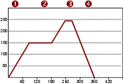
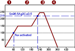
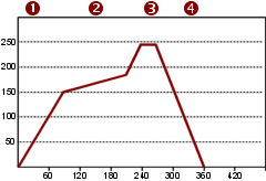
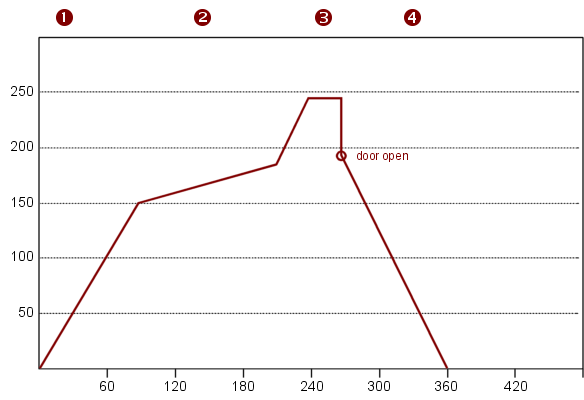
Profile characteristics
The standard reflow profile has four zones: preheat, soak, reflow and cooling. The profile describes the ideal temperature curve of the top layer of the PCB.
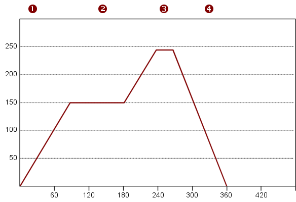
Standard reflow soldering profile
 The preheating zone should increase the temperature at a maximum rate of
3 °C/s. The purpose of preheating is to allow the solvents to evaporate
and to activate the flux.
The preheating zone should increase the temperature at a maximum rate of
3 °C/s. The purpose of preheating is to allow the solvents to evaporate
and to activate the flux.
 The soak zone brings the temperature of all components and board areas to an
equal level. Due to differences in thermal inertia, components do not heat up at
the same speed —this is especially the case with infra-red heating, due
to uneven absorption of infra-red energy by components (depending on colour and
reflectivity).
The soak zone brings the temperature of all components and board areas to an
equal level. Due to differences in thermal inertia, components do not heat up at
the same speed —this is especially the case with infra-red heating, due
to uneven absorption of infra-red energy by components (depending on colour and
reflectivity).
 In the reflow zone, the temperature rises at a rate of approximately 2 °C
to a temperature above the melting point (the temperature above liquidus,
or TAL). The peak temperature for the reflow zone is at least 25 °C
above TAL, because solder both coalesces better with the copper and wets
the pads and component pins better when it is hotter —thereby creating
better joints. This is especially important for lead-free solders (SAC305),
because this solder is less effective at wetting than leaded solders.
In the reflow zone, the temperature rises at a rate of approximately 2 °C
to a temperature above the melting point (the temperature above liquidus,
or TAL). The peak temperature for the reflow zone is at least 25 °C
above TAL, because solder both coalesces better with the copper and wets
the pads and component pins better when it is hotter —thereby creating
better joints. This is especially important for lead-free solders (SAC305),
because this solder is less effective at wetting than leaded solders.
The TAL (temperature above liquidus) should be held for 40 to 80 seconds, so that an intermetallic compound (IMC) is able to form. Note that the duration of the reflow zone is shorter than the TAL period, because the temperature is still above liquidus at the start of the cooling zone.
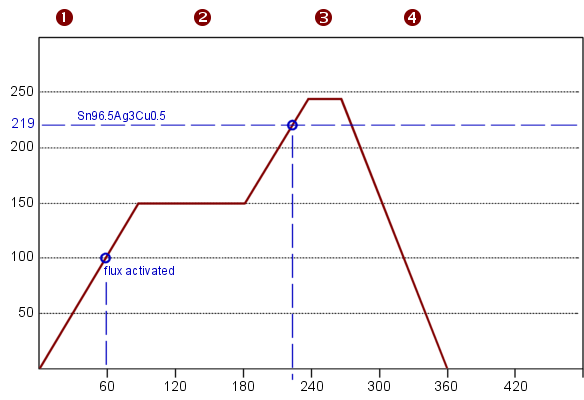
Decision points in a profile
 The cooling zone ideally has a ramp of 4 °C/s (to cool down
quickly, but avoid thermal stress). Free air cooling is sufficient.
The cooling zone ideally has a ramp of 4 °C/s (to cool down
quickly, but avoid thermal stress). Free air cooling is sufficient.
The flux in the solder paste gets activated at approximately 100 °C. After it is activated, the TAL should be reached within roughly 3 minutes — or less for no-clean solder paste, as as these pastes have less active flux. Exceeding that time deteriorates the effectiveness of the flux. In other words, the flux in the solder paste sets an upper bound on the duration of the soak zone.
Refining the soak zone

Profile with a slanted soak phase
For lead-free reflow soldering, a disadvantage of the standard profile is the relative height of the peak of the reflow zone. With the soak zone at 150 °C and the reflow zone at 245 °C (typical value for lead-free reflow soldering), the temperature rise from soak zone to reflow zone is 95 °C. Due to thermal inertia, such a large quick temperature rise may, again, lead to temperature differences across the PCB. Rather than increasing the temperature of the soak zone on the whole, an alternative profile is to make the soak zone temperature a slow ramp from 150 °C to 180 °C. The lower relative peak of the reflow zone results in a more equalized temperature across the PCB and components.
As written above, you may want to reduce the duration of the soak zone, especially when using no-clean solder paste (no-clean paste has less active flux). The optimal duration of the soak zone also depends on the PCB, therefore some experimentation is recommended.
Refining the reflow zone
During reflow, an “intermetallic compound” forms where the tin touches the pads on the PCB. The forming of this intermetallic compound (IMC), which consists primarily of copper and tin, is a requirement for a good solder joint; the speed at which it forms is a function of the temperature.
Although the forming of the IMC is a requirement for a good solder joint, excessive growth should be avoided. The copper/tin intermetallic compound is brittle and therefore the larger it grows, the greater the risks for cracks when the joint is point under stress —such as stress due to the repeated expansion and contraction of components that warm up and cool down during their operational life).
For (lead-free) reflow soldering, the advised soldering temperature is 245 °C, which is well below the advised temperature of a soldering iron for hand soldering. The rationale for this advise is that the intermetallic compound grows more slowly at lower temperatures, and therefore avoids excessive growth. If, for a particular PCB, it turns out that the cold spots have not been sufficiently heated for a proper reflow, the advise is to lengthen the reflow zone (but keep the peak temperature at 245 °C).
As an aside: with hand soldering (using a soldering iron), the “time above liquidus” (TAL) of the solder is much shorter than during reflow, and therefore a higher soldering temperature is admissible.
With the eC-reflow-mate, the reflow duration can be set in two ways: either by adjusting the points in the profile curve, or by enabling and setting the “reflow hold time” option. With both methods, the oven starts holding the temperature when it reaches the reflow temperature (typically set at 245 °C); the difference between the two options is the start of the cool-down phase. When using the profile, the cool-down phase starts at the time in the profile; when using the “reflow hold time” option, cool-down starts the specified number of seconds since first reaching the reflow temperature. The reflow hold option is often easier to use and it gives better control over the total reflow period.
Refining the cool zone
Cooldown phase
As with many batch ovens, the eC-reflow-mate has a slow cool-down temperature ramp. To cool down more quickly, the oven opens the door at some pre-set temperature; this temperature should be chosen so that the solder is guaranteed to have solidified. The default temperature setting for this is 190 °C (for lead free soldering); this is on the safe side, for many boards the door-open temperature can be increased to 195–200 °C.
The temperature ramp for cooling down is largely dictated by thermal inertia and the decision to open the door is determined by the PCB temperature (the highest value measured by the three sensors is used for the decision whether to open the door). Therefore, the time set for cooling down is barely relevant. It is common practice to set the cool-down period up to opening the door to be just 1 second. The ramp for cooling down with the door open is irrelevant as well: the PCB is subject to free air cooling.
Bottom heating
The eC-reflow-mate has heaters on the top and the bottom and these are individually controlled. The bottom heater helps to reduce the difference between hot spots and cold spots on the PCB. For PCBs with components only on a single side, the bottom temperature can be made equal to the top temperature (“Follow 0 °C”). For PCBs with components on both sides, the bottom heater can either be set to follow the top heater at -40 °C, or to be set to a fixed temperature of approximately 180 °C.
Profile recommendations
The table below is a starting point for a profile for a batch oven. The optimal profile also depends on the PCB, and therefore the suitability of a profile must be verified with actual measurements.
| Zone | Lead (Sn63 Pb37) | Lead-free (SAC305) |
|---|---|---|
| Preheat | to 150 °C in 60 s | to 150 °C in 60 s |
| Soak | from 150 °C to 165 °C in 120 s | from 150 °C to 180 °C in 120 s |
| Reflow | Peak temperature 225 °C to 235 °C, hold for 20 s | Peak temperature 245 °C to 255 °C, hold for 15 s |
| Cooling | -4 °C/s or free-air cooling | -4 °C/s or free-air cooling |
It should be verified (by measurements) that the peak temperature does not exceed the specifications of the components (in both temperature and the period at this temperature), and that the duration of temperature above liquidus is in a 40 s to 80 s window.
Ideal profile versus measured profile
To give an indication of a temperature profile in practice, here is a screen shot of the software for the eC-reflow-mate, with the prescribed profile superimposed. In this graphic, the red curve represents a sensor that floats above the PCB, the yellow curve is for the sensor the floats below the PCB, the green curve represent a sensor that touches the PCB and the blue curve is the prescribed profile.
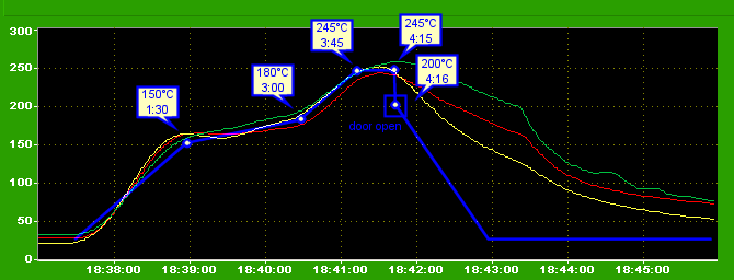
Clearly visible is the effect of thermal inertia and how the eC-reflow-mate compensates for it by overshooting the target curve (see for example the yellow curve near 1:30 from the start). Also visible is how the PCB is still heating up while the oven itself is already cooling down (see the green curve near 4:15 from the start). The PCB cools down slowly, until the door opens —which happens when the green curve reaches 200 °C.
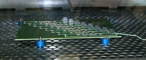
PCB spacers (stand-offs)
The curves correspond to a PCB with a size of 100×150mm that was put on PCB spacers in the middle of the oven (see the image at the right). The bottom heating is set to follow the top heating (“Follow 0 °C”).
Closing remarks
Different kinds of PCBs need different profiles. This application note assumes PCBs from common FR4 material. For power electronics, and notably power LEDs, PCBs based on “Insulated Metal Substrate” (IMS) are often used. IMS consists of a metal carrier (usually aluminium) with a thin epoxy-based layer glued on top of it and an etched copper layer for the circuit on the epoxy layer. By necessity, IMS PCBs are single-sided circuits with only traces on the top layer (the “component” layer), and they are only suitable for surface-mount components (SMDs). For the solder profile, the main characteristic of IMS is that aluminium has low thermal inertia and good thermal conductivity. The temperature differences are minimal across the board (no hot spots versus cold spots). The soak zone can therefore be shortened (or be removed altogether).
Most reflow ovens can run as an independent, self-contained unit. All reflow ovens that we are aware of, can be monitored with a computer. We advise to monitor the temperature curves and to check these against the profile —even if no problematic solder joints have surfaced. We also advise you to keep logs of the reflow runs, both for successful and unsuccessful runs, so that these can be compared and analysed. For example, following up on the measured graph (pictured above), we subsequently compensated for the slow cool-down after reflow by reducing the reflow time in the profile from 30 seconds to 10 seconds (since the measured time above liquidus turned out to be easily 30 seconds longer than the prescribed reflow time —for this PCB).
Further reading
- Lee, Dr. Ning-Chen, Optimizing Reflow Progile via Defect Mechanisms Analysis, Soldering and Surface Mount Technology, vol. 11 nr. 1, 1999.
- A survey of the effects of temperature and duration of various zones on the solderability and the quality of solder joints. The conclusions are only partially relevant for the eC-reflow-mate, because the paper assumes the use of forced convection ovens (Although the eC-reflow-mate has a ventilator to create air flow, it behaves primarily as an infra-red oven.) .
- Peo, Marc, How Challenging Conventional Wisdom Can Optimize Solder Reflow, Surface Mount Technology Magazine (Pennwell Corp.), May 1998.
- This article focuses on six conventional wisdoms. It discusses the new perspectives brought by modern reflow ovens and modern solder pastes.
- J-STD-020D.1, JEDEC, March 2008
- A joint IPC/JEDEC standard on the moisture/reflow classification of SMD devices. Though oft cited, note that the standard prescribes the profile in section 5.6 for the purpose of classification of components. It is not necessarily suitable as a production profile. In particular, the recommended hold time of the temperature above liquidus of 60 to 150 seconds, is far longer than other recommendations.
